In the realm of modern electronics, where precision and efficiency reign supreme, the quest for superior materials and manufacturing techniques is unending. Among the myriad of components that constitute the backbone of electronic devices, printed circuit boards (PCBs) stand as fundamental pillars. These intricate platforms serve as the very foundation upon which electronic circuits are built, enabling the seamless flow of electrical signals. In this pursuit of excellence, one innovation has emerged as a cornerstone in the domain of PCB fabrication: the Alumina Multi-Layered Board by Etching.
The Alumina Multi-Layered Board (AMLB) represents a pinnacle of engineering ingenuity, combining the remarkable properties of alumina with the intricacy of multi-layered design. Through the meticulous process of etching, this technology achieves unprecedented levels of performance, reliability, and miniaturization, catering to the evolving demands of diverse industries ranging from telecommunications to aerospace.
Unveiling the Alumina Advantage
At the heart of the AMLB lies alumina, a ceramic material renowned for its exceptional electrical insulation, thermal conductivity, and mechanical robustness. With its high dielectric strength and low loss tangent, alumina ensures minimal signal attenuation and distortion, making it an ideal substrate for high-frequency applications. Moreover, its superior thermal properties facilitate efficient heat dissipation, crucial for maintaining the integrity and longevity of electronic components, especially in demanding environments.
The Art of Layering: Multi-Layered Design
Central to the functionality of AMLBs is their multi-layered architecture, a feat of design engineering that enables the integration of complex circuits within a compact footprint. Unlike conventional single-layer or double-layer boards, AMLBs feature multiple layers interconnected through vias, allowing for enhanced routing density and signal integrity. This multi-layered approach not only optimizes space utilization but also mitigates issues such as signal crosstalk and electromagnetic interference (EMI), critical considerations in high-speed and high-frequency applications.
Precision Engineering: The Etching Process
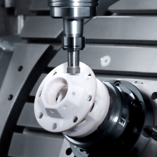
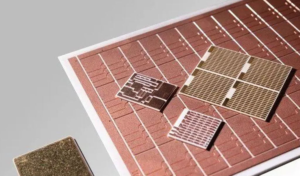
At the core of AMLB fabrication lies the intricate process of etching, a technique that epitomizes precision engineering. Etching involves selectively removing material from the surface of a substrate to create intricate patterns and circuits. In the case of AMLBs, this process is carried out on layers of alumina ceramic coated with a thin film of conductive material, typically copper. Through a combination of chemical etchants and patterning techniques such as photolithography, the desired circuitry is etched onto the substrate with unparalleled accuracy and repeatability.
Unraveling the Etching Process: A Step-by-Step Guide
1. Substrate Preparation:
The process begins with the preparation of alumina substrates, which are meticulously cleaned and inspected to ensure uniformity and purity. Any imperfections or contaminants could compromise the integrity of the final product, making substrate preparation a critical step in the etching process.
2. Application of Photoresist:
Next, a layer of photoresist is applied to the surface of the alumina substrate. Photoresist is a light-sensitive material that acts as a mask during the etching process, protecting certain areas of the substrate while allowing others to be etched away. The application of photoresist is typically achieved through spin coating or spray coating, followed by a curing process to harden the material.
3. Photolithography:
Once the photoresist is applied, the substrate undergoes photolithography, a process that involves exposing it to ultraviolet (UV) light through a photomask. The photomask contains the desired circuit patterns, which are transferred onto the photoresist upon exposure to UV light. Areas of the photoresist exposed to UV light become soluble and are subsequently washed away, revealing the underlying alumina substrate.
4. Etching:
With the circuit patterns defined on the substrate, the etching process can commence. Metal Etching is typically carried out using chemical etchants that selectively dissolve the exposed areas of the substrate, leaving behind the desired circuit traces. Common etchants for alumina substrates include acidic solutions such as hydrochloric acid or alkaline solutions such as sodium hydroxide, depending on the specific requirements of the application.
5. Resist Stripping:
Once the etching process is complete, the remaining photoresist is stripped away to reveal the final circuitry. This is typically achieved through a combination of solvent immersion and mechanical agitation, ensuring complete removal of the photoresist without damaging the underlying substrate or circuit traces.
Advantages of AMLB by Etching
1. High Density Integration:
By leveraging the multi-layered design enabled by etching, AMLBs offer unparalleled routing density, allowing for the integration of complex circuits within a compact footprint. This high-density integration is essential for miniaturization and space-constrained applications, where traditional PCBs may fall short.
2. Enhanced Signal Integrity:
The precision and accuracy of the etching process ensure minimal line width and spacing tolerances, thereby enhancing signal integrity and reducing the risk of signal distortion or crosstalk. This is particularly crucial in high-speed and high-frequency applications, where even minor deviations can have significant repercussions.
3. Superior Thermal Management:
Thanks to the thermal properties of alumina, AMLBs exhibit excellent heat dissipation capabilities, mitigating the risk of thermal-induced failures and ensuring the reliability and longevity of electronic components. This makes them well-suited for applications operating in harsh environments or under elevated temperatures.
4. Customization and Flexibility:
The versatility of the etching process allows for the customization of AMLBs to meet the specific requirements of diverse applications. Whether it’s complex circuitry, specialized materials, or unique form factors, AMLBs can be tailored to suit a wide range of applications, offering unparalleled flexibility and versatility.
Applications Across Industries
1. Telecommunications:
In the realm of telecommunications, where high-speed data transmission and reliability are paramount, AMLBs find widespread use in devices such as routers, switches, and base stations. Their high-frequency performance, compact form factor, and robust construction make them ideal for supporting the ever-increasing demands of modern communication networks.
2. Aerospace and Defense:
In the aerospace and defense sector, where ruggedness, reliability, and miniaturization are critical, AMLBs play a pivotal role in a myriad of applications, including radar systems, avionics, and missile guidance systems. Their ability to withstand extreme temperatures, shock, and vibration, coupled with their high-density integration capabilities, make them indispensable in mission-critical environments.
3. Medical Devices:
In the field of medical devices, where precision, reliability, and biocompatibility are paramount, AMLBs are utilized in a variety of applications ranging from diagnostic equipment to implantable devices. Their ability to deliver high-performance electronics in a compact and lightweight package makes them ideal for applications where space is limited, such as wearable health monitors and implantable medical devices.
Future Perspectives and Challenges
As the demand for high-performance electronics continues to escalate, the evolution of AMLBs by etching is poised to accelerate further. Advancements in materials science, manufacturing techniques, and design methodologies are expected to unlock new frontiers in miniaturization, performance, and functionality, paving the way for a new era of electronic innovation.
However, along with these opportunities come inherent challenges, ranging from cost considerations to technical complexities. The high precision and specialized equipment required for AMLB fabrication can pose barriers to entry for smaller manufacturers, while the ever-increasing demands for faster speeds and higher densities present ongoing engineering challenges.
Conclusion
In the ever-evolving landscape of electronic engineering, the Alumina Multi-Layered Board by Etching stands as a testament to human ingenuity and innovation. Through the seamless integration of advanced materials, precision manufacturing techniques, and intricate design methodologies, AMLBs have redefined the boundaries of what is possible in electronic circuitry.
From telecommunications to aerospace, from medical devices to consumer electronics, the impact of AMLBs is felt across a myriad of industries, driving progress and propelling innovation forward. As we stand on the brink of a new era of electronic advancement, one thing is certain: the Alumina Multi-Layered Board by Etching will continue to shape the future of electronics, ushering in a world of endless possibilities.